| Sapphire Nitro+ Radeon RX 6900 XT SE (Rev 2.0) | EVGA GeForce RTX 3080 Ti FTW3 Ultra Hybrid Gaming | |
363 W + 21 % + 21 % |
Max TDP | 350 W |
| NA | Consumo energetico giornaliero (kWh) | NA |
| NA | Costo di esercizio al giorno | NA |
| NA | Consumo di energia all'anno (kWh) | NA |
| NA | Costo di esercizio all'anno | NA |
Sapphire Nitro+ Radeon RX 6900 XT SE (Rev 2.0) vs EVGA GeForce RTX 3080 Ti FTW3 Ultra Hybrid Gaming
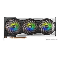
Sapphire Nitro+ Radeon RX 6900 XT SE (Rev 2.0) ha lanciato Q2/2021, che si basa sull'architettura AMD Radeon RX 6900 XT. Verrà fornito con 16 GB di memoria GDDR6 ad alta larghezza di banda.Il Sapphire Nitro+ Radeon RX 6900 XT SE (Rev 2.0) dispone di 5120 shader, 128 unità di output di rendering, ha un boost clock di 2.365 GHz+ 5 % e dotato di un 363 W+ 21 % . La GPU supporta fino a 4 monitor con risoluzioni di 7680x4320 . Inoltre, se stai cercando un Air cooling raffreddamento Axial e un tipo di ventola Axial, sarebbe la scelta migliore.
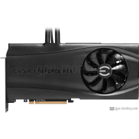
EVGA GeForce RTX 3080 Ti FTW3 Ultra Hybrid Gaming ha lanciato Q2/2021, che si basa sull'architettura NVIDIA GeForce RTX 3080 Ti. Verrà fornito con 12 GB di memoria GDDR6X ad alta larghezza di banda.Il EVGA GeForce RTX 3080 Ti FTW3 Ultra Hybrid Gaming dispone di 10240 shader, 96 unità di output di rendering, ha un boost clock di 1.800 GHz+ 8 % e dotato di un 350 W . La GPU supporta fino a 4 monitor con risoluzioni di 7680x4320 . Inoltre, se stai cercando un AIO water cooling raffreddamento Axial e un tipo di ventola Axial, sarebbe la scelta migliore.
Sapphire Nitro+ Radeon RX 6900 XT SE (Rev 2.0)
EVGA GeForce RTX 3080 Ti FTW3 Ultra Hybrid Gaming
Confronta dettaglio
GPU |
||
| AMD Radeon RX 6900 XT | Based on | NVIDIA GeForce RTX 3080 Ti |
| Navi 21 | GPU Chip | GA102-225-A1 |
| 80 | Unità di esecuzione | 80 |
| 5120 | Shader | 10240 |
| 128 | Render Output Units | 96 |
| 320 | Texture Units | 320 |
Memory |
||
| 16 GB | Memory Size | 12 GB |
| GDDR6 | Memory Type | GDDR6X |
| 2 GHz | Memory Speed | 1.188 GHz |
| 512 GB/s | Memory Bandwith | 912 GB/s |
| 256 bit | Memory Interface | 384 bit |
Clock Speeds |
||
| 1.825 GHz | Base Clock | 1.365 GHz |
| 2.365 GHz+ 5 % |
Boost Clock | 1.800 GHz+ 8 % |
| 2.135 GHz+ 6 % |
Avg (Game) Clock | |
|
Yes |
Overclocking |
Yes |
Thermal Design |
||
| 363 W+ 21 % |
TDP | 350 W |
| 390 W+ 13 % |
TDP (up) | -- |
| -- | Tjunction max | 93 °C |
| 1 x 6-Pin, 2 x 8-Pin | PCIe-Power | 3 x 8-Pin |
Cooler & Fans |
||
| Axial | Fan-Type | Axial |
| 3 x 100 mm | Fan 1 | 1 x 100 mm |
| -- | Fan 2 | 2 x 120 mm |
| Air cooling | Cooler-Type | AIO water cooling |
| 0 dB / Silent | Noise (Idle) | 0 dB / Silent |
| -- | Noise (Load) | -- |
Connectivity |
||
| 4 | Max. Displays | 4 |
| 2.3 | HDCP-Version | 2.3 |
| 1x HDMI v2.1 | HDMI Ports | 1x HDMI v2.1 |
| 3x DP v1.4a | DP Ports | 3x DP v1.4a |
| -- | DVI Ports | -- |
| -- | VGA Ports | -- |
| -- | USB-C Ports | -- |
Featureset |
||
| 7680x4320 | Max. resolution | 7680x4320 |
| 12_2 | DirectX | 12_2 |
| Yes |
Raytracing | Yes |
| No |
DLSS / FSR | Yes} |
| Addressable LED | LED | Addressable LED |
Supported Video Codecs |
||
| Decode / Encode | h264 | Decode / Encode |
| Decode / Encode | h265 / HEVC | Decode / Encode |
| Decode |
AV1 | Decode |
| Decode / Encode | VP8 | Decode |
| Decode / Encode | VP9 | Decode |
Dimensions |
||
| 310 mm | Length | 289 mm |
| 134 mm | Height | 138 mm |
| 55 mm | Width | 42 mm |
| 3 PCIe-Slots | Width (Slots) | 3 PCIe-Slots |
| -- | Weight | -- |
| PCIe 4.0 x 16 | GPU Interface | PCIe 4.0 x 16 |
Additional data |
||
| 11308-03-20G | Part-no | -- |
| Q2/2021 | Data di rilascio | Q2/2021 |
| -- | Release price | -- |
| 7 nm | Structure size | 8 nm |
| data sheet | Documents | data sheet |

Stima dell'utilizzo elettrico

Stima dell'utilizzo elettrico
Confronto popolare
Sapphire Toxic Radeon RX 6900 XT Extreme Edition vs
Sapphire Nitro+ Radeon RX 6900 XT SE (Rev 2.0)
Sapphire Nitro+ Radeon RX 6900 XT SE (Rev 2.0) vs
EVGA GeForce RTX 3080 Ti FTW3 Ultra Gaming
Sapphire Nitro+ Radeon RX 6900 XT SE (Rev 2.0) vs
ASUS TUF GAMING Radeon RX 6900 XT OC
GIGABYTE AORUS GeForce RTX 3080 Xtreme 10G vs
Sapphire Nitro+ Radeon RX 6900 XT SE (Rev 2.0)
Sapphire Nitro+ Radeon RX 6900 XT SE (Rev 2.0) vs
ZOTAC Gaming GeForce RTX 3080 Ti AMP Holo
Sapphire Nitro+ Radeon RX 6900 XT SE (Rev 2.0) vs
ASUS ROG Strix LC Radeon RX 6900 XT TOP
Sapphire Nitro+ Radeon RX 6900 XT SE (Rev 2.0) vs
PowerColor Red Devil Radeon RX 6900 XT
Sapphire Nitro+ Radeon RX 6900 XT SE (Rev 2.0) vs
XFX Speedster MERC 319 Radeon RX 6900 XT Black Gaming
Sapphire Nitro+ Radeon RX 6900 XT SE (Rev 2.0) vs
EVGA GeForce GTX 1660 XC OC
Sapphire Nitro+ Radeon RX 6900 XT SE (Rev 2.0) vs
PowerColor Liquid Devil Radeon RX 6900 XT Ultimate
MSI Radeon RX 6900 XT Gaming Z Trio 16G vs
Sapphire Nitro+ Radeon RX 6900 XT SE (Rev 2.0)
MSI GeForce RTX 3080 Ti Ventus 3X 12G OC vs
Sapphire Nitro+ Radeon RX 6900 XT SE (Rev 2.0)
Sapphire Nitro+ Radeon RX 6900 XT SE (Rev 2.0) vs
PowerColor Red Devil Radeon RX 6900 XT Ultimate
ZOTAC Gaming GeForce RTX 3080 AMP Holo vs
Sapphire Nitro+ Radeon RX 6900 XT SE (Rev 2.0)
Sapphire Nitro+ Radeon RX 6900 XT SE (Rev 2.0) vs
MSI Radeon RX 5700 Evoke GP
Sapphire Nitro+ Radeon RX 6900 XT SE (Rev 2.0) vs
EVGA GeForce RTX 3080 Ti FTW3 Ultra Hybrid Gaming
Sapphire Nitro+ Radeon RX 6900 XT SE (Rev 2.0) vs
Sapphire Nitro+ Radeon RX 6900 XT
Sapphire Nitro+ Radeon RX 6900 XT SE (Rev 2.0) vs
MSI Radeon RX 6800 XT Gaming X Trio 16G
Sapphire Nitro+ Radeon RX 6900 XT SE (Rev 2.0) vs
Sapphire Nitro+ Radeon RX 6900 XT SE
GALAX GeForce RTX 3070 Ti EX White (1-Click OC) vs
Sapphire Nitro+ Radeon RX 6900 XT SE (Rev 2.0)
AMD Radeon RX 6900 XT vs
Sapphire Nitro+ Radeon RX 6900 XT SE (Rev 2.0)
Sapphire Nitro+ Radeon RX 6900 XT SE (Rev 2.0) vs
Sapphire Nitro+ Radeon RX 6800 XT SE
ASUS TUF Gaming GeForce RTX 3080 Ti OC vs
Sapphire Nitro+ Radeon RX 6900 XT SE (Rev 2.0)
Sapphire Nitro+ Radeon RX 6900 XT SE (Rev 2.0) vs
MSI Radeon RX 5700 XT Evoke OC
Sapphire Nitro+ Radeon RX 6900 XT SE (Rev 2.0) vs
INNO3D GeForce RTX 2070 SUPER TWIN X2 OC
EVGA GeForce RTX 3080 Ti FTW3 Ultra Hybrid Gaming vs
EVGA GeForce RTX 3080 Ti XC3 Ultra Hybrid Gaming
EVGA GeForce RTX 3080 Ti FTW3 Ultra Hybrid Gaming vs
ASUS ROG Strix LC GeForce RTX 3080 Ti OC
EVGA GeForce RTX 3080 Ti FTW3 Ultra Hybrid Gaming vs
GIGABYTE AORUS GeForce RTX 3080 Ti Xtreme 12G
MSI GeForce RTX 3080 Ti Suprim X 12G vs
EVGA GeForce RTX 3080 Ti FTW3 Ultra Hybrid Gaming
EVGA GeForce RTX 3080 Ti FTW3 Ultra Hybrid Gaming vs
ASUS ROG Strix GeForce RTX 3090 OC
EVGA GeForce RTX 3080 Ti FTW3 Ultra Gaming vs
EVGA GeForce RTX 3080 Ti FTW3 Ultra Hybrid Gaming
ZOTAC Gaming GeForce RTX 3080 Ti AMP Holo vs
EVGA GeForce RTX 3080 Ti FTW3 Ultra Hybrid Gaming
EVGA GeForce RTX 3090 FTW3 ULTRA HYBRID GAMING vs
EVGA GeForce RTX 3080 Ti FTW3 Ultra Hybrid Gaming
EVGA GeForce RTX 3080 Ti FTW3 Ultra Hybrid Gaming vs
ASUS TUF Gaming GeForce RTX 3080 Ti OC
GALAX GeForce RTX 2080 White (1-Click OC) vs
EVGA GeForce RTX 3080 Ti FTW3 Ultra Hybrid Gaming
EVGA GeForce RTX 3080 Ti FTW3 Ultra Hybrid Gaming vs
MSI GeForce RTX 3090 Gaming Trio 24G
EVGA GeForce RTX 3080 Ti FTW3 Ultra Hybrid Gaming vs
GALAX GeForce RTX 2080 Dual Black
ASUS ROG Strix LC Radeon RX 6900 XT TOP vs
EVGA GeForce RTX 3080 Ti FTW3 Ultra Hybrid Gaming
Sapphire Nitro+ Radeon RX 6900 XT SE (Rev 2.0) vs
EVGA GeForce RTX 3080 Ti FTW3 Ultra Hybrid Gaming
EVGA GeForce RTX 3080 Ti FTW3 Ultra Hybrid Gaming vs
SAPPHIRE PULSE Radeon RX 6700 XT
INNO3D GeForce GTX 1060 iCHILL Black 6GB vs
EVGA GeForce RTX 3080 Ti FTW3 Ultra Hybrid Gaming
MSI GeForce RTX 3090 Gaming X Trio 24G vs
EVGA GeForce RTX 3080 Ti FTW3 Ultra Hybrid Gaming
GIGABYTE GeForce RTX 3080 Ti Gaming OC 12G vs
EVGA GeForce RTX 3080 Ti FTW3 Ultra Hybrid Gaming
ASUS TUF Gaming GeForce RTX 3080 Ti vs
EVGA GeForce RTX 3080 Ti FTW3 Ultra Hybrid Gaming
EVGA GeForce RTX 3080 Ti FTW3 Ultra Hybrid Gaming vs
Colorful iGame GeForce RTX 3060 Ti Vulcan OC LHR-V
EVGA GeForce RTX 3080 Ti FTW3 Ultra Hybrid Gaming vs
EVGA GeForce RTX 3090 XC3 ULTRA HYBRID GAMING
EVGA GeForce RTX 3080 Ti FTW3 Ultra Hybrid Gaming vs
MSI GeForce RTX 3090 Suprim X 24G
EVGA GeForce RTX 3080 Ti FTW3 Ultra Hybrid Gaming vs
NVIDIA GeForce RTX 3090 Founders Edition
EVGA GeForce RTX 3080 Ti FTW3 Ultra Hybrid Gaming vs
NVIDIA GeForce RTX 3060 Ti Founders Edition
EVGA GeForce RTX 3080 Ti FTW3 Ultra Hybrid Gaming vs
EVGA GeForce RTX 2080 SUPER FTW3 Hybrid Gaming